
DDS信号发生器的设计
DDS信号发生器的设计(任务书,开题报告,外文翻译,论文14000字)
摘 要
在数字通信系统中,一种全新的频率合成技术直接数字频率合成技术(DDS)以它独有的特点被广泛采用。可编程逻辑器件可以通过现场编程来改变电路,简化了数字电路系统的设计,缩小了数字电路系统的体积,并且提高了数字电路系统的灵活性和可靠性,非常适合用来实现DDS。
本文设计实现了一个DDS信号发生器:首先将波形ROM数据存储在FPGA本身的RAM中,通过对时钟信号进行分频和相位累加,得到当前相位值,然后对输出波形进行调用ROM数据存储。再经高速数模转换,低通滤波器后输出所需函数信号。本文设计了系统硬件电路,利用QuartusII作为软件开发平台,利用Verilog 语言设计程序,利用ModelSim进行软件仿真,最后进行软硬联调测试系统性能。
利用FPGA开发板结合外围扩展电路作为系统硬件平台,本文实现了正弦波、三角波、方波的可调输出,且波形频率、幅度可变。也证明了采用软硬件结合的方式,通过对FPGA的编程实现DDS设计的可行性和可靠性。
关键词:DDS FPGA 信号发生器
The design of DDS signal generator
Abstract
As a kind of new frequency synthesis technology,direct digital frequency synthesis technology (DDS) is widely used in digital communication system. Field programmable logic devices can be programmed to change the circuit, this greatly simplifies the design of digital circuit system, reducing the size of the digital circuit system, and improve the flexibility and reliability of digital circuit system, very suitable for used to realize DDS.
This design implements a DDS signal generator. First, the waveform data stored in the RAM of the FPGA itself, through the clock signal frequency and phase accumulation, waveform output by calling ROM storage, and then through the high-speed D / A converter, low-pass filter output function signal. This paper presents the system hardware circuit, QuartusII use as a software development platform, using Verilog language design ModelSim simulation software. Finally, hard and soft joint commissioning to test system performance.
Using FPGA development board and peripheral expansion circuit as a hardware platform realizing adjustable output sine, triangle, square wave in this paper, and the waveform frequency, amplitude variable, also it demonstrated the use of a combination of software and hardware, based on the FPGA programming to realize the feasibility and reliability of the design of DDS.
Key Words: DDS; FPGA; Signal Generator


目录
摘 要 I
Abstract II
第一章 绪论 1
1.1 课题背景及意义 1
1.2 国内外信号发生器的发展现状 1
1.3 论文主要工作与章节安排 2
第二章 理论研究 3
2.1 DDS基本原理与构成 3 [版权所有:http://DOC163.com]
2.1.1 DDS原理 3
2.1. 2 DDS基本结构 4
2.2 四分之一波形存储原理 5
2.3 本章小结 6
第三章 设计方案论证 7
3.1 FPGA开发板论证与比较 7
3.2 ROM查找表方案论证 7
3.3 键盘显示方案论证 8
3.4 数模转换方案论证 8
3.5 滤波方案论证 8
3.6 本章小结 9
第四章 硬件设计 10
4.1 信号发生器硬件结构 10
4.2 FPGA主控电路 10
4.2.1 IO引脚 11
4.2.2 时钟电路 11
4.2.3 配置电路 11
4.3 数模转换电路 12
4.4 二阶有源低通滤波器 14
4.5 键盘电路 15
4.6 显示单元电路 16
4.7 本章小结 17
[资料来源:http://www.doc163.com]
第五章 软件设计 18
5.1 软件平台QuartusII介绍 18
5.2 波形数据生成 18
5.2.1 正弦波的数据采样 18
5.2.2 三角波的数据采样 19
5.2.3 方波的数据采样 21
5.3 DDS的Verilog实现 22
5.3.1 波形ROM 22
5.3.2 整体设计 23
5.3.3 顶层模块 23
5.3.4 APP模块 24
5.3.5 DDS模块 25
5.3.6 LCD1602模块 27
5.3.7 键盘模块 29
5.4 本章小结 31
第六章 结果与分析 32
6.1 软件仿真 32
6.2 软硬件综合调试 34
6.2.1 硬件测试 34
6.2.2 软硬联调 35
第七章 总结与展望 38 [资料来源:https://www.doc163.com]
7.1 总结 38
7.2 展望 38
参考文献 40
致谢 42
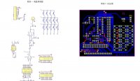
附录一 电路原理图 43
附录二 PCB图 44
附录三 源程序 45 [资料来源:http://www.doc163.com]